
Plenary Speakers
![]() Download Plenary Speakers Program (PDF)
Download Plenary Speakers Program (PDF)
Plenary Speakers Presentation Schedule |
||
| Monday October 15th |
8:20 am |
Jesus del Alamo Massachusetts Institute of Technology Nanoscale III-V Electronics: InGaAs FinFETs and Vertical Nanowire MOSFETs |
|
9:10 am |
Ian A. Young Intel Corporation Beyond CMOS Materials and Devices for Energy Efficient Computing |
|
| Tuesday October 16th |
8:20 am |
Kaustav Banerjee UC Santa Barbara 2D Materials for Smart Life |
|
9:10 am |
Joseph M. Luther National Renewable Energy Laboratory Metal Halide Perovskites at the Nanoscale: high quality optoelectronic materials with unique phase properties |
|
| Wednesday October 17th |
8:20 am |
Nadar Engheta, Nanotechnology Council Pioneer Award Winner University of Pennsylvania Near-Zero-Index Photonic Materials and Devices |
|
9:10 am |
Tony F. Heinz Stanford University Optical properties of 2D materials and heterostructures |
|

Director of the Microsystems Technology Laboratories
Donner Professor and Professor of Electrical Engineering
Department of Electrical Engineering and computer Science
Massachusetts Institute of Technology
Cambridge, MA, USA
Topic: “Nanoscale III-V Electronics: InGaAs FinFETs and Vertical Nanowire MOSFETs”
Jesús A. del Alamo, Xin Zhao, Wenjie Lu, Alon Vardi and Xiaowei Cai
Microsystems Technology Laboratories, Massachusetts Institute of Technology
Abstract:
In the last few years, as Si electronics faces mounting difficulties to maintain its historical scaling path, III-V compound semiconductors, in particular InGaAs, have received a great deal of attention. Sub-10 nm CMOS applications require a 3D transistor geometry. In this regard, the vertical nanowire (VNW) MOSFET represents the ultimate scalable transistor. The gate-all-around nanowire configuration allows for the greatest degree of charge control in the channel. The vertical transport direction uncouples footprint scaling (on the plane of the wafer) from gate length scaling (normal to the wafer) leading to the best possible combination of transistor density and short-channel effects.
At MIT, we are investigating vertical nanowire InGaAs MOSFETs and FinFETs fabricated by a top-down approach. Towards this goal, we have developed Reactive Ion Etching technology for In-containing III-V compounds that yields high aspect ratio structures with vertical and smooth sidewalls. We have also perfected digital etch to controllably thin down fins and vertical nanowires to below 10 nm width/diameter. Using these technologies, we have demonstrated InGaAs VNW MOSFETs and FinFETs with sub-10 nm critical dimensions. In both families of transistors, we have obtained promising electrical characteristics. This talk will review these recent developments, put them in context of the overall progress of Si CMOS and outline the prospects and challenges of III-V transistors for future nanoscale logic.
Speaker Biography:
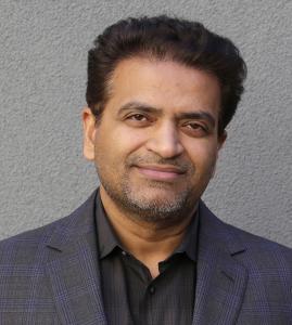
Jesús A. del Alamo is the Director of the Microsystems Technology Laboratories at Massachusetts Institute of Technology. He obtained a Telecommunications Engineer degree from the Polytechnic University of Madrid and MS and PhD degrees in Electrical Engineering from Stanford University. From 1985 to 1988 he was with NTT LSI Laboratories in Atsugi (Japan) and since 1988 he has been with the Department of Electrical Engineering and Computer Science of MIT where he currently is the Donner Professor. His current research interests are centered on nanoelectronics based on compound semiconductors for future logic, communications and power management applications. Prof. del Alamo was an NSF Presidential Young Investigator. He is a member of the Royal Spanish Academy of Engineering and Fellow of the IEEE and the APS. He has received the Intel Outstanding Researcher Award, the SRC Technical Excellence Award, and the IEEE EDS Education Award.
Professor, Electrical and Computer Engineering
Nanoelectronics Research Lab, UC Santa Barbara
Topic: “2D Materials for Smart Life”
Abstract:
Two-dimensional (2D) materials such as graphene and various transition metal dichalcogenides (such as MoS2) possess a wide range of remarkable properties that make them attractive for a number of applications, including sub-10 nm VLSI. I will highlight the prospects of 2D materials for innovating energy-efficient transistors, sensors, interconnects and passive devices targeted for next-generation electronics needed to support the emerging paradigm of the Internet of Things (IoT). More specifically, I will bring forward a few applications uniquely enabled by 2D materials and their heterostructures that have been demonstrated in my lab for realizing ultra-energy-efficient electronics. This will include the world’s first Kinetic Inductor that exploits a low-dimensional material property of graphene to overcome a 200 years old limitation of the conventional Faraday-inductor and opens up a new pathway for designing ultra-compact IoT systems (Nature Electronics 2018), a 2D-channel band-to-band tunneling transistor that overcomes a fundamental power consumption challenge in all electronic devices since the invention of the first transistor (Nature 2015), the first 2D FET based biosensor with unprecedented sensitivity (ACS Nano 2014), as well as a breakthrough interconnect technology based on doped-graphene-nanoribbons, which overcomes the fundamental limitations of conventional metals and provides an attractive pathway toward an energy-efficient and highly reliable interconnect technology for next-generation integrated circuits (Nano Letters 2017). I will also discuss the prospects of monolithic 3D integration with 2D materials for realizing 3D ICs of ultimate thinness and integration density.
Speaker Biography:
Professor Kaustav Banerjee from UC Santa Barbara is one of the world’s leading innovators in the field of nanoelectronics. His current research focuses on the physics, technology, and applications of van der Waals materials and heterostructures for next-generation electronics, photonics, and bioelectronics. Initially trained as a physicist, he graduated from UC Berkeley with a PhD in electrical engineering in 1999. Professor Banerjee is a Fellow of IEEE, American Physical Society (APS), Japan Society for the Promotion of Science (JSPS), and the American Association for the Advancement of Science (AAAS). Professor Banerjee’s contributions to energy-efficient electronics, including seminal work on interconnects, 3D ICs, and thermal-aware VLSI design, have been recognized by the IEEE with a Technical Field Award (2015 Kiyo Tomiyasu Award), one of the institute’s highest honors, as well as the prestigious Bessel Prize in 2011 from the Humboldt Foundation.
2018 Nanotechnology Council Pioneer Award Winner
H. Nedwill Ramsey Professor
of Electrical and Systems Engineering
and
Professor of Physics and Astronomy
University of Pennsylvania
Philadelphia, Pennsylvania, USA
Topic: “Near-Zero-Index Photonic Materials and Devicesc
Abstract:
Metamaterials and metasurfaces have enabled scientists and technologists with unique tools to tailor and manipulate waves in unconventional ways, providing novel platforms with unprecedented wave physics and engineering for photonic materials, optical devices and components. One such platform is the near-zero-index photonics. In such media, the effective relative permittivity and/or relative permeability is engineered to be very low (i.e. near zero) at the operating frequency, which leads to the near-zero effective refractive index. As a result, in such epsilon-near-zero (ENZ), mu-near-zero (MNZ), and/or near-zero-index (NZI) structures the wavelength is “stretched”, and consequently the phase distribution is effectively uniform throughout the structure’s volume. A variety of unique phenomena including supercoupling, photonic doping, electric levitation, extreme quantum optics, thermal beaming, and giant nonlinearity is exhibited in such platforms. In this talk, I will present an overview of some of our results in these areas, and will discuss some of their potential applications.
Speaker Biography:
Nader Engheta is the H. Nedwill Ramsey Professor at the University of Pennsylvania in Philadelphia, with affiliations in the Departments of Electrical and Systems Engineering, Bioengineering, Materials Science and Engineering, and Physics and Astronomy. He received his B.S. degree from the University of Tehran and his M.S and Ph.D. degrees from Caltech. His current research activities span a broad range of areas including photonics, metamaterials, nano-optics, graphene optics, electrodynamics, imaging and sensing inspired by eyes of animal species, microwave and optical antennas, and physics and engineering of fields and waves. He has received several awards for his research including the 2017 William Streifer Scientific Achievement Award from the IEEE Photonics Society, the 2015 Gold Medal from SPIE, the 2015 Fellow of US National Academy of Inventors (NAI), the 2014 Balthasar van der Pol Gold Medal from the International Union of Radio Science (URSI), the 2017 Beacon of Photonics Industry Award from the Photonics Media, the 2015 Vannevar Bush Faculty Fellowship Award from US Department of Defense, the 2012 IEEE Electromagnetics Award, the 2015 IEEE Antennas and Propagation Society Distinguished Achievement Award, the 2015 Wheatstone Lecture in King’s College London, the 2013 Inaugural SINA Award in Engineering, 2006 Scientific American Magazine 50 Leaders in Science and Technology, the Guggenheim Fellowship, and the IEEE Third Millennium Medal. He is a Fellow of seven international scientific and technical organizations, i.e., IEEE, OSA, APS, MRS, SPIE, URSI, and American Association for the Advancement of Science (AAAS).He has received the honorary doctoral degrees from the Aalto University in Finland in 2016, the University of Stuttgart, Germany in 2016, and Ukraine’s National Technical University Kharkov Polytechnic Institute in 2017.

Professor of Applied Physics and Photon Science at Stanford University, Stanford, CA USA
Associate Laboratory Director for Energy Sciences at the SLAC National Accelerator Laboratory.
Topic: “Optical properties of 2D materials and heterostructures”
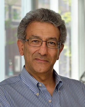
Tony Heinz is a Professor of Applied Physics and Photon Science at Stanford University and the Associate Laboratory Director for Energy Sciences at the SLAC National Accelerator Laboratory. Heinz received a BS degree in Physics from Stanford University and a PhD degree, also in Physics, from UC Berkeley in 1982. He was subsequently at the IBM Research Division in Yorktown Heights, NY until he joined Columbia University in 1995 as a Professor of Electrical Engineering and Physics. At Columbia, he served as a Scientific Director of the Columbia Nanoscale Science and Engineering Center (NSEC) and of the Energy Frontier Research Center (EFRC). He was the President of the Optical Society of America in 2012. Heinz joined Stanford in 2015.
Heinz’s research has centered on the elucidation of the properties and dynamics of nanoscale materials primarily through the application of optical and laser techniques. His research on surfaces, interfaces, and nanoscale materials, including carbon nanotubes, graphene and other 2D materials, has been recognized by Optics Prize of the International Commission for Optics, a Research Award of the von Humboldt Foundation, the Julius Springer Prize for Applied Physics, and the Isakson Prize of the American Physical Society.
Senior Scientist, National Renewable Energy Laboratory, Golden, CO, USA.
Topic: “Metal Halide Perovskites at the Nanoscale: high quality optoelectronic materials with unique phase properties”
Abstract:
The newly rediscovered perovskite semiconductor system has the potential to be extremely transformative for all optoelectronic devices, especially photovoltaics (PVs). Perovskite semiconductors of the form APbI3 where A is a large +1 charged cation, typically Cs, methylammonium, or formamidinium have had a huge resurgence among materials scientists for outstanding PV properties despite being overlooked for decades. Semiconductors containing the latter two A-site cations listed are hybrid organic-inorganic materials, and as such, are far less understood compared to conventional all inorganic or even organic material systems. Regardless of this spotty formal understanding, lead-halide perovskites have very rapidly been optimized to power conversion efficiency levels on par with all other materials even with extensive history of research. Perovskites show a unique tolerance to crystalline defects that cause trouble in most other semiconductors. Therefore the potential offered is that very high efficiency PVs can be fabricated in extremely fast and inexpensive ways, thus offering a revolution for the solar industry and a direct route toward producing the world’s energy with a simple and clean technology. Long-term durability of the devices is the critical remaining challenge to be solved.1 Two examples of major instabilities in device performance are the volatility of the organic cation and the specific crystal habit in which the material embodies.
Nanoscale versions (often termed quantum dots (QDs)) of the all-inorganic metal halide perovskite (CsPbI3) tend to retain the desired cubic phase due to strain effects at the surface of the QDs whereas conventional films of the same material “relax” to an orthorhombic structure at room temperature. Therefore these QDs potentially solve both of the instability issues. The cubic CsPbI3 QD cells operate with a rather remarkable open-circuit voltage of >1.2 volts and have produced power conversion efficiencies over 13%.2,3 This customizable new nanomaterial system has incredible potential for many applications in optoelectronics, including photovoltaics, LEDs, displays and lasers. We describe the formation of α-CsPbI3 QD films with long range electronic transport that retain the high temperature phase in ambient conditions making up the active layer in optoelectronic devices. Perspectives on how this technology can become transformative will be discussed.
References
- A. Christians, P. Schulz, J.S. Tinkham, T.H. Schloemer, S.P. Harvey, B.J .Tremolet de Villers, A. Sellinger, J.J. Berry, J.M. Luther, Nature Energy, 2018, 3 (1), 68.
- Swarnkar, A.R. Marshall, E.M. Sanehira, B.D. Chernomordik, D.T. Moore, J.A. Christians, T. Chakrabarti, J.M. Luther, Science, 2016, 354 (6308), 92-95.
- M. Sanehira, A.R. Marshall, J.A. Christians, S.P. Harvey, P.N. Ciesielski, L.M. Wheeler, P. Schulz, L.Y. Lin, M.C. Beard, J.M. Luther, Science Advances, 2017, 3 (10), eaao4204.
Speaker Biography:
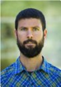
Joseph Luther is a senior scientist at the National Renewable Energy Laboratory in Golden, CO, USA. He received his PhD in Physics from Colorado School of Mines in 2008 for his work on colloidal PbS and PbSe quantum dot solar cells for multiple exciton generation, where one photon can generate multiple electron hole pairs, thus leading to solar cells that can outperform the existing SQ limit of 32%. After postdoctoral training at UC Berkeley under mentor Paul Alivisatos, he rejoined NREL in 2009. He published over 80 peer-reviewed papers regarding solution processed solar cells. Current research focuses on perovskite solar cells and semiconductor nanocrystals.
 Ian A. Young
Intel Senior Fellow,
Technology and Manufacturing Group
Director, Exploratory Integrated Circuits,
Intel Corporation,
Hillsboro, Oregon, USA
Topic: “Beyond CMOS Materials and Devices for Energy Efficient Computing”
Abstract:
An analysis of research in quantum materials for beyond CMOS devices (nanoelectronic and/or nanomagnetic) is presented. Some device proposals and demonstrations are reviewed and trends in this field are identified. Considerations guiding development of competitive computing technologies are described. Results of beyond-CMOS circuit benchmarking are reviewed.
Speaker Biography:
Ian Young is a Senior Fellow and director of Exploratory Integrated Circuits in the Technology and Manufacturing Group of Intel Corporation. He joined Intel in 1983 and his technical contributions have been in the design of DRAMs, SRAMs, microprocessor circuit design, Phase Locked Loops and microprocessor clocking, mixed-signal circuits for microprocessor high speed I/O links, RF CMOS circuits for wireless transceivers, and research for chip to chip optical I/O. He has also contributed to the definition and development of Intel’s process technologies. He now leads a research group exploring the future options for the integrated circuit in the beyond CMOS era.
Ian Young received the Bachelor of Electrical Engineering and the Master Eng. Science, from the University of Melbourne, Australia. He received the PhD in Electrical Engineering from the University of California, Berkeley. He is the recipient of the 2009 International Solid-State Circuits Conference’s Jack Raper Award for Outstanding Technology Directions paper. He received the 2018 IEEE Frederik Philips Award “for leadership in research and development on circuits and processes for the evolution of microprocessors”. Ian Young is a Fellow of the IEEE.